Gas detector
Researchers at MIT have built a chip-based optical device that dynamically controls incoming infrared light.
It acts as a tunable lens for infrared cameras used in chemical sensing, thermal imaging and pollution monitoring.
Each microscopic pixel of the device's lens can be controlled independently.
This lets the device change its focus and detect different signals without moving parts, a feature that current infrared sensing systems generally lack.
The work is described in a paper published in Nature Communications.
The team also built a lab-scale demonstration using mostly conventional semiconductor manufacturing processes, an indication that the approach could eventually be produced at industrial scale.
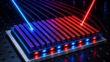
The device is built around a metasurface: a material patterned with structures fine enough to control how light passes through it.
The system works in the mid-infrared wavelength range, which the human eye cannot see but which many organic molecules absorb.
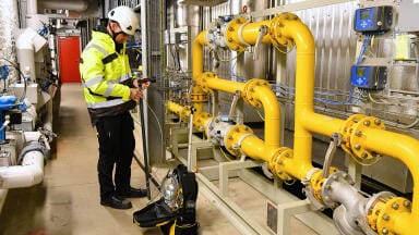
That property already underpins gas detection instruments used to spot methane and propane leaks, and to monitor chemical compounds in the atmosphere.
Cosmin-Constantin Popescu, the paper's first author and an MIT PhD graduate, said the technology could support environmental monitoring directly.
"This could give us more information as we study space, or help with environmental protections where you want to monitor for specific compounds in the atmosphere," Popescu said.
"Thermal imaging is another application... Basically, a lot of organic molecules absorb in the mid-infrared wavelength, and you could use this system to detect them."
Juejun Hu, MIT's John F. Elliott Professor of Materials Science and Engineering and a principal investigator on the project, has previously worked with metasurfaces built from phase-change materials, which shift between solid and liquid states when heated.
That phase change alters how the material interacts with light.
An earlier device from Hu's group, reported in 2021, could adjust its focus to different depths, but only across the whole material at once. The new work set out to control light independently at each microscopic pixel instead.
"Most active metasurfaces trying to do single-pixel tuning need wires going to every pixel, and how you route the wires becomes a big issue," Hu said.
"The best approach so far has been one-dimensional pixel control with a bunch of wires."
To solve that, the researchers adapted a crossbar architecture already used in displays, in which two perpendicular layers of copper wires sit above a layer of doped silicon.
The silicon generates heat at each crossing point of the wires, switching the phase-change material beneath it between crystalline and amorphous states, and so changing how each pixel handles incoming infrared light.
A diode selector at each pixel prevents unintended current from leaking into neighbouring pixels.
"We did some calculations showing this architecture allows us to scale to potentially millions of pixels without having any issues with the [unintended] currents," Hu said.
It is the first time anyone has implemented two-dimensional pixel-level control for active phase-change metasurfaces, he added.
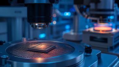
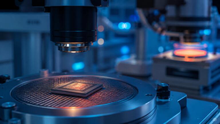
Working with equipment at MIT.nano and with a semiconductor chip factory, the team produced a two-dimensional metasurface with a six-by-six pixel array. The array switched on and off reliably during testing.
"We found this mesh architecture to be very resilient," Popescu said.
"You don't want these materials to switch once and not work anymore. You want it to switch a large number of times: maybe tens of thousands of times or more."
The researchers argue that using semiconductor foundry manufacturing, rather than a one-off research process, is what will let the design move beyond a lab prototype.
"As you want to scale up, you need something that's part of a consistent process, and that's why chip foundry manufacturing becomes so important," Hu said. "Working with a semiconductor foundry with well-defined process control is very powerful."
The team is now working to add more pixels to the array and to make the system more durable.
The aim is to capture more infrared information relevant to a given application, such as configuring the device to highlight a specific chemical signature.
Hu also noted that metasurfaces have separately been used to emulate the computational structure of neural networks, an application he said remains some way from practical use but could eventually support new approaches to optical computing.
The work was supported, in part, by the US Air Force, the National Science Foundation, the National Research Foundation of Korea, and the Draper Scholar Program.
PIN 27.4 Aug/Sept 2026




 Product directory